USB 3.1 Type-C Solderable Connectors (10-Pack)
Official Store Deal
Expert Analysis Overview
Introduction: The Precision of Modern Connectivity
The USB 3.1 Type-C Solderable Connectors are precision-engineered components designed for electronics repair technicians and DIY enthusiasts seeking to integrate or restore modern connectivity in custom projects and damaged devices. These small Boards represent a critical bridge, allowing for the revitalization of expensive gadgets or the creation of bespoke electronics where a robust, reversible USB-C interface is paramount. Many modern devices, from smartphones to laptops and specialized industrial equipment, rely heavily on the versatile Type-C standard for both power and data. When a port fails due to physical damage, wear and tear, or manufacturing defects, the entire device often becomes unusable. This necessitates a component-level repair. Replacing a faulty port on a motherboard or designing a custom peripheral from scratch demands a connector that offers both electrical integrity and mechanical stability. These connectors provide exactly that, offering a cost-effective alternative to full board replacement. They are not merely replacement parts for a quick fix. They are enablers of innovation and repair, extending the lifespan of valuable electronics and fostering creativity in custom builds.Anatomy of a Connection: Design and Build Quality
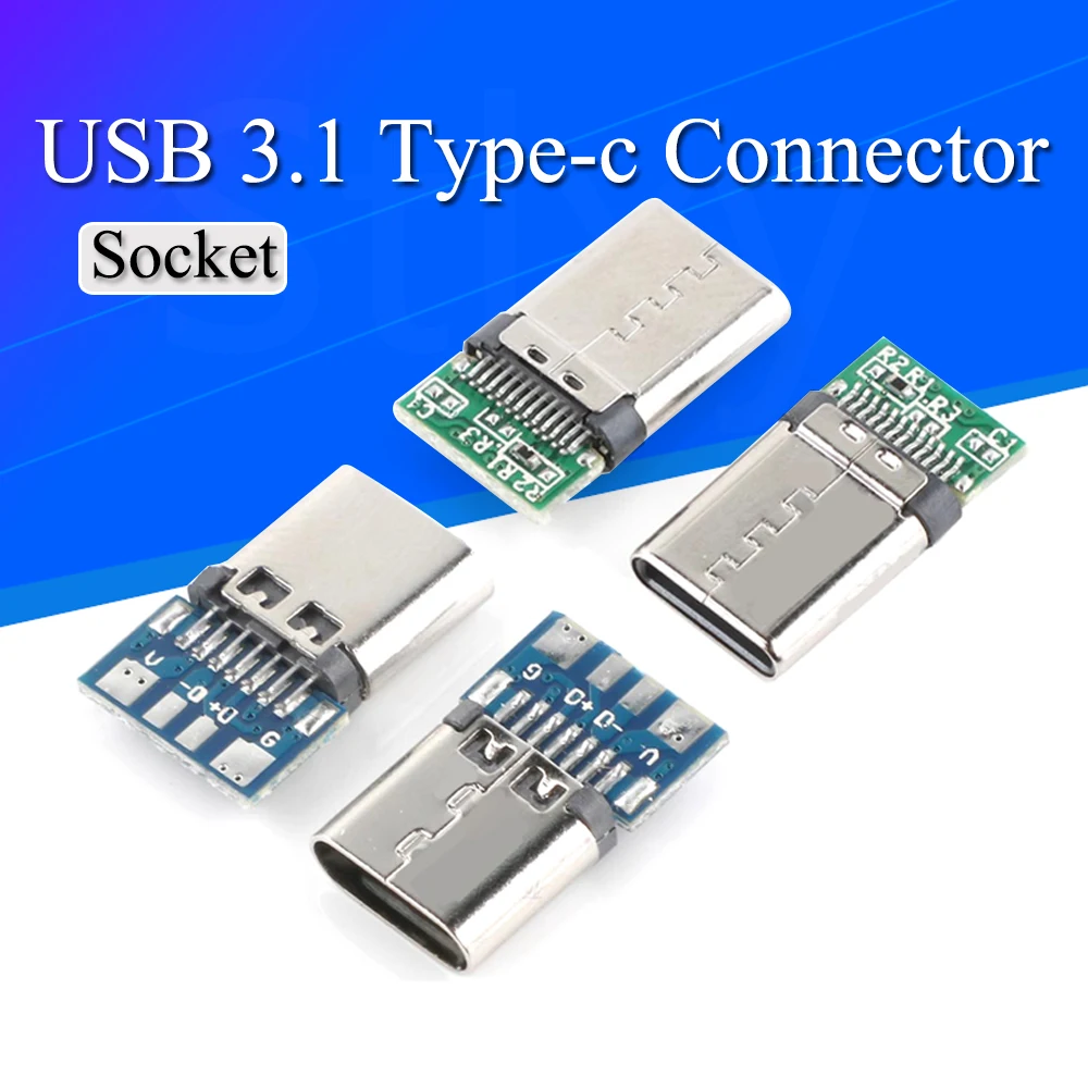
The physical construction of these USB 3.1 Type-C connectors immediately conveys their purpose: reliable integration into complex circuits. Each unit features a robust metal housing that encases the intricate 24-pin connector itself. This metal shell serves multiple critical functions. It provides essential EMI (Electromagnetic Interference) shielding, a crucial element for maintaining signal integrity, especially at the high data transfer rates associated with USB 3.1. Without proper shielding, external electromagnetic fields could corrupt data or introduce noise into the system. The metal housing also offers significant mechanical protection, safeguarding the delicate internal pins from physical impact and repeated insertions. This enhances the longevity of the connection point. It resists physical impact.The connector is securely mounted onto a compact PCB breakout board. This board, typically observed in a vibrant green or deep blue hue, is fabricated from an FR-4 substrate. FR-4 is a widely recognized and reliable material for printed circuit boards, known for its good electrical insulation properties and mechanical strength. The choice of FR-4 ensures a stable and durable platform for soldering, resisting warping under heat. Unlike older, more fragile USB connectors like Micro-USB or Mini-USB, the Type-C standard is inherently more durable due to its symmetrical, reversible design. This eliminates the frustration and potential damage caused by incorrect insertion attempts. The 24-pin configuration on these specific connectors ensures full compliance with the USB 3.1 specification. This means comprehensive support for all the advanced features the standard offers, including up to 10 Gbps data transfer speeds. Imagine transferring gigabytes of high-resolution video files or large software installations in mere seconds, a task that would crawl on older USB 2.0 interfaces. This speed is a significant leap from the theoretical 480 Mbps offered by USB 2.0. It is a major upgrade. The breakout board itself is thoughtfully designed with clearly labeled solder pads for each of the 24 pins, simplifying the often-complex task of identifying individual connections. This meticulous labeling, visible even under moderate magnification, is a boon for any technician or hobbyist, drastically reducing the chances of miswiring.
The Art of Integration: Soldering and Prototyping
The primary utility of these connectors lies in their solderable nature, making them ideal for component-level work rather than simple plug-and-play applications. They are raw components intended for permanent, secure integration into a circuit board or custom cable assembly. The small PCB acts as an essential intermediary, effectively breaking out the tiny, closely spaced pins of the Type-C connector into larger, more manageable solder pads. This design greatly eases the soldering process. This eases soldering. It transforms a highly intricate task into something achievable with standard fine-tip soldering equipment. Without this breakout board, directly soldering to the connector's minuscule pins would be an exercise in extreme micro-soldering, often requiring specialized hot-air rework stations and advanced magnification.Consider a scenario where a custom embedded system, perhaps a smart home hub or a specialized data logger, requires a modern, high-speed interface for configuration and power. These connectors are ideal. Their compact footprint allows for seamless integration into tight enclosures, a common constraint in custom electronics. The clearly marked pads for VBUS (power), GND (ground), D+ and D
Beyond the Basics: Performance and Versatility
These USB 3.1 Type-C connectors are not just about establishing a physical connection; they are about enabling a suite of advanced capabilities inherent to the modern USB-C standard. The USB 3.1 standard, specifically Gen 2, allows for impressive data transfer rates of up to 10 Gigabits per second (Gbps). This substantial bandwidth is critical for a wide array of demanding applications, including the rapid transfer of large multimedia files, streaming high-resolution video to external displays, or connecting high-speed external solid-state drives (SSDs) that require maximum throughput. The full 24-pin layout, unlike simplified 16-pin versions, also inherently supports USB Power Delivery (PD). For those unfamiliar with this crucial specification, USB PD is a protocol that allows for higher power transfer, potentially up to 100W, over a single USB-C cable. This means a single, reversible cable can handle both high-speed data and significant power for charging power-hungry devices like laptops, or powering demanding industrial sensors.Compared to generic, older USB 2.0 connectors, which are limited to 480 Mbps and typically 5V/0.5A, these Type-C connectors offer a substantial upgrade in both speed and power capabilities. Imagine the convenience of charging a laptop directly from a custom-built power bank or a specialized solar charging array, all through a single, robust connection. This is entirely possible with proper PD implementation in the surrounding circuitry. The versatility of these connectors extends further to supporting various Alternate Modes, such as DisplayPort or HDMI over USB-C, provided the connected circuitry and host device are designed to handle these specific protocols. This opens up possibilities for custom video output solutions or specialized docking stations. Possibilities are vast. The reversible nature of the Type-C connector itself is a significant user experience enhancement. There is no "wrong way" to plug it in, which not only reduces user frustration but also minimizes wear and tear on the port and the cable over time. This small detail contributes significantly to the long-term reliability of the connection. It improves reliability.
Addressing the Challenges: Skill and Precision
While these connectors offer immense utility and advanced features, their successful implementation hinges directly on the user's technical proficiency. Soldering these small components, particularly the closely spaced pins on the breakout board, requires a steady hand, excellent eyesight, and prior experience with fine-pitch soldering techniques. The individual solder pads are quite small. Misalignment, excessive heat, or an unsteady hand can easily lead to undesirable outcomes such as bridged connections between pins, cold solder joints, or even irreversible damage to the delicate PCB traces. This is unequivocally not a task recommended for novice solderers without proper practice. However, for those with the requisite skills and tools, the value proposition is compelling. Instead of facing the prohibitive cost and complexity of replacing an entire motherboard due to a damaged USB-C port, a skilled technician can precisely replace just the faulty connector. This approach saves significant money, reduces electronic waste, and effectively extends the operational life of valuable electronics. This saves money.A notable design consideration, which can be viewed as a minor trade-off, is the lack of integrated strain relief directly on the breakout board itself. Unlike some pre-assembled cables that incorporate molded plastic strain relief, these bare components require the user to engineer their own solutions. This is particularly important for custom cables that will experience frequent flexing or movement. A simple application of epoxy potting around the soldered connections or the design of a custom 3D-printed enclosure can provide the necessary mechanical support. This prevents undue stress on the delicate solder joints and ensures long-term reliability, even under dynamic conditions. These are considerations that an experienced builder will naturally account for in their project planning.
The Long-Term View: Durability and Reliability
The long-term durability and reliability of the final USB-C connection largely depend on two critical factors: the quality of the initial soldering work and the subsequent mechanical protection applied. The metal housing of the connector itself is inherently robust, designed to resist physical wear and tear from hundreds, if not thousands, of repeated insertions and removals. It resists physical wear. However, the solder joints connecting the breakout board to the main circuit are the most vulnerable points. Proper soldering techniques, which include adequate flux application, precise temperature control, and sufficient solder wetting, are paramount. A well-executed solder joint will appear shiny, smooth, and concave, forming a strong electrical and mechanical bond that can withstand environmental stresses. Conversely, a dull, lumpy, or convex joint (a "cold joint") will be prone to intermittent connections and eventual failure.Regular inspection of these connections is advisable, especially for devices deployed in high-vibration environments, such as robotics or automotive applications. The compact nature of these components means they can be integrated discreetly into almost any project. This is a major advantage for custom designs where space is at a premium. Picture a perfectly repaired smartphone, its USB-C port functioning flawlessly, indistinguishable from its original state. This component makes that level of restoration possible. The initial investment in these high-quality connectors, coupled with the necessary skill, pays significant dividends in extended device life, enhanced functionality, and the satisfaction of a job well done. They are built to last, provided they are installed correctly. They are built to last.